LTC4261/LTC4261-2
29
42612fc
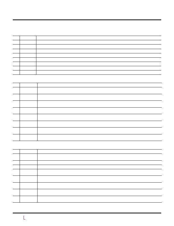
Table 3. STATUS Register A (00h)Read Only
BIT
NAME
OPERATION
A7
FET On
Indicates State of FET; 1 = FET On, 0 = FET Off
A6
PGIO Input
Indicates State of the PGIO Pin when Configured to General Purpose Input: 1 = PGIO High, 0 = PGIO Low
A5
FET Short
Indicates Potential FET Short if Current Sense Voltage Exceeds 2mV While FET is Off; 1 = FET is Shorted, 0 = FET is Not Shorted
A4
EN
Indicates State of the EN Pin; 1 = EN Pin High, 0 = EN Pin Low
A3
Power Bad
Indicates Power is Bad when PGI is High at the End of the PGI Check Timer; 1 = PGI High, 0 = PGI Low
A2
Overcurrent
Indicates Overcurrent Condition; 1 = Overcurrent, 0 = Not Overcurrent
A1
Undervoltage Indicates Input Undervoltage when Both UVH and UVL are Low; 1 = UVH and UVL Low, 0 = UVH or UVL High
A0
Overvoltage
Indicates Input Overvoltage when OV is High; 1 = OV High, 0 = OV Low
Table 4. FAULT Register B (01h)Read/Write
BIT
NAME
OPERATION
B7
External Fault
Occurred
Latched to 1 if FLTIN Goes Low; 1 = FLTIN Low State Detected, 0 = FLTIN has Not Been Low
B6
PGIO Input
High Occurred
Latched to 1 if the PGIO Pin Goes High when Configured to General Purpose Input; 1 = PGIO High Detected,
0 = PGIO has Been Low
B5
FET Short Fault
Occurred
Indicates Potential FET Short was Detected When Measured Current Sense Voltage Exceeded 2mV While FET was Off;
1 = FET Short Fault Occurred, 0 = No FET Short Fault
B4
EN Changed
State
Indicates That a Board was Inserted or Extracted when EN Changed State; 1 = EN Changed State, 0 = EN Unchanged
B3
Power Bad
Fault Occurred
Indicates Power was Bad when PGI was High at the End of the PGI Check Timer; 1 = Power Bad Fault Occurred,
0 = No Power Bad Fault
B2
Overcurrent
Fault Occurred
Indicates Overcurrent Fault Occurred; 1 = Overcurrent Fault Occurred, 0 = No Overcurrent Fault
B1
Undervoltage
Fault Occurred
Indicates Input Undervoltage Fault Occurred when Both UVH and UVL went Low; 1 = Undervoltage Fault Occurred,
0 = No Undervoltage Fault
B0
Overvoltage
Fault Occurred
Indicates Input Overvoltage Fault Occurred when OV was High; 1 = Overvoltage Fault Occurred, 0 = No Overvoltage Fault
Table 5. ALERT Register C (02h)Read/Write
BIT
NAME
OPERATION
C7
External Fault
Alert
Enables Alert for External Fault When FLTIN was Low; 1 = Enable Alert, 0 = Disable Alert (Default)
C6
PGIO Output
Output Data Bit to PGIO Pin when Configured as Output. Defaults to 0
C5
FET Short Alert Enables Alert for FET Short Fault; 1 = Enable Alert, 0 = Disable Alert (Default)
C4
EN State
Change Alert
Enables Alert when EN Changed State; 1 = Enable Alert, 0 Disable Alert (Default)
C3
Power Bad
Alert
Enables Alert for Power Bad Fault; 1 = Enable Alert, 0 Disable Alert (Default)
C2
Overcurrent
Alert
Enables Alert for Overcurrent Fault; 1 = Enable Alert, 0 Disable Alert (Default)
C1
Undervoltage
Alert
Enables Alert for Undervoltage Fault; 1 = Enable Alert, 0 Disable Alert (Default)
C0
Overvoltage
Alert
Enables Alert for Overvoltage Fault; 1 = Enable Alert, 0 Disable Alert (Default)
APPLICATIONS INFORMATION
发布紧急采购,3分钟左右您将得到回复。
相关PDF资料
LTC4263IS#TRPBF
IC IEEE 803.2AF CNTRLR 14-SOIC
LTC4268IDKD-1#PBF
IC PD HIGH POWER W/CNTRL 32-DFN
LTC4274CUHF#PBF
IC CONTROLLER POE 38-QFN
LTC4280CUFD#PBF
IC CONTROLLER HOT SWAP QFN-24
LTC4300-1IMS8#TRPBF
IC HOTSWAP 2WIRE BUS BUFFR 8MSOP
LTC4300A-2IMS8#TRPBF
IC BUFFER BUS 2WR HOTSWAP 8-MSOP
LTC4301IDD
IC BUFFER BUS HOTSWAP 2WR 8DFN
LTC4301LIDD#TRPBF
IC BUFFER BUS HOTSWAP 2WR 8DFN
相关代理商/技术参数
LTC4261IGN-2#TRPBF
功能描述:IC CTRLR HOTSWAP W/ADC 28-SSOP RoHS:是 类别:集成电路 (IC) >> PMIC - 热交换 系列:- 产品培训模块:Lead (SnPb) Finish for COTS
Obsolescence Mitigation Program 标准包装:119 系列:- 类型:热交换控制器 应用:通用型,PCI Express? 内部开关:无 电流限制:- 电源电压:3.3V,12V 工作温度:-40°C ~ 85°C 安装类型:表面贴装 封装/外壳:80-TQFP 供应商设备封装:80-TQFP(12x12) 包装:托盘 产品目录页面:1423 (CN2011-ZH PDF)
LTC4261IUFD
功能描述:IC CTRLR HOTSWAP W/ADC 24-QFN RoHS:否 类别:集成电路 (IC) >> PMIC - 热交换 系列:- 产品培训模块:Lead (SnPb) Finish for COTS
Obsolescence Mitigation Program 标准包装:119 系列:- 类型:热交换控制器 应用:通用型,PCI Express? 内部开关:无 电流限制:- 电源电压:3.3V,12V 工作温度:-40°C ~ 85°C 安装类型:表面贴装 封装/外壳:80-TQFP 供应商设备封装:80-TQFP(12x12) 包装:托盘 产品目录页面:1423 (CN2011-ZH PDF)
LTC4261IUFD#PBF
功能描述:IC CTRLR HOTSWAP W/ADC 24-QFN RoHS:是 类别:集成电路 (IC) >> PMIC - 热交换 系列:- 产品培训模块:Lead (SnPb) Finish for COTS
Obsolescence Mitigation Program 标准包装:119 系列:- 类型:热交换控制器 应用:通用型,PCI Express? 内部开关:无 电流限制:- 电源电压:3.3V,12V 工作温度:-40°C ~ 85°C 安装类型:表面贴装 封装/外壳:80-TQFP 供应商设备封装:80-TQFP(12x12) 包装:托盘 产品目录页面:1423 (CN2011-ZH PDF)
LTC4261IUFD#TR
功能描述:IC CTRLR HOTSWAP W/ADC 24-QFN RoHS:否 类别:集成电路 (IC) >> PMIC - 热交换 系列:- 产品培训模块:Lead (SnPb) Finish for COTS
Obsolescence Mitigation Program 标准包装:119 系列:- 类型:热交换控制器 应用:通用型,PCI Express? 内部开关:无 电流限制:- 电源电压:3.3V,12V 工作温度:-40°C ~ 85°C 安装类型:表面贴装 封装/外壳:80-TQFP 供应商设备封装:80-TQFP(12x12) 包装:托盘 产品目录页面:1423 (CN2011-ZH PDF)
LTC4261IUFD#TRPBF
功能描述:IC CTRLR HOTSWAP W/ADC 24-QFN RoHS:是 类别:集成电路 (IC) >> PMIC - 热交换 系列:- 产品培训模块:Lead (SnPb) Finish for COTS
Obsolescence Mitigation Program 标准包装:119 系列:- 类型:热交换控制器 应用:通用型,PCI Express? 内部开关:无 电流限制:- 电源电压:3.3V,12V 工作温度:-40°C ~ 85°C 安装类型:表面贴装 封装/外壳:80-TQFP 供应商设备封装:80-TQFP(12x12) 包装:托盘 产品目录页面:1423 (CN2011-ZH PDF)
LTC4261IUFD-2
制造商:LINER 制造商全称:Linear Technology 功能描述:Negative Voltage Hot Swap Controllers with ADC and I2C Monitoring
LTC4261IUFD-2#PBF
功能描述:IC CTRLR HOTSWAP W/ADC 24-QFN RoHS:是 类别:集成电路 (IC) >> PMIC - 热交换 系列:- 产品培训模块:Lead (SnPb) Finish for COTS
Obsolescence Mitigation Program 标准包装:119 系列:- 类型:热交换控制器 应用:通用型,PCI Express? 内部开关:无 电流限制:- 电源电压:3.3V,12V 工作温度:-40°C ~ 85°C 安装类型:表面贴装 封装/外壳:80-TQFP 供应商设备封装:80-TQFP(12x12) 包装:托盘 产品目录页面:1423 (CN2011-ZH PDF)
LTC4261IUFD-2#TRPBF
功能描述:IC CTRLR HOTSWAP W/ADC 24-QFN RoHS:是 类别:集成电路 (IC) >> PMIC - 热交换 系列:- 产品培训模块:Lead (SnPb) Finish for COTS
Obsolescence Mitigation Program 标准包装:119 系列:- 类型:热交换控制器 应用:通用型,PCI Express? 内部开关:无 电流限制:- 电源电压:3.3V,12V 工作温度:-40°C ~ 85°C 安装类型:表面贴装 封装/外壳:80-TQFP 供应商设备封装:80-TQFP(12x12) 包装:托盘 产品目录页面:1423 (CN2011-ZH PDF)
